|
|
| (26 intermediate revisions by 6 users not shown) |
| Line 1: |
Line 1: |
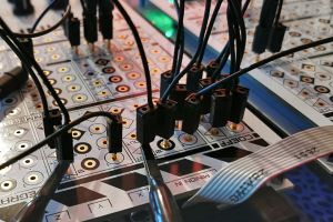
| − | '''The Analog Thing''' (abbreveated as ''THAT'') is a small analog computer built for educational and recreational purposes by [[anabrid GmbH]]. The computer will be available for sale at the net cost of its components, i.e. as cheap as possible and not-for-profit. We are targeting a retail price of around EUR150. The component list, circuit diagrams and circuit board layouts of this computer are released as Open Source, and information on how to build it from scratch and how to operate it will be released here on this wiki. | + | [[File:Cta bg.jpg|thumb|A closeup of a THAT in [[Minion]] mode with [[Oscilloscope]] probes attached.]] |
| | + | '''The Analog Thing''' (abbreviated as ''THAT'') is a high-quality, low-cost, open-source, and not-for-profit cutting-edge analog computer developed by [[anabrid]] under the brand Analog Paradigm for educational and recreational purposes. THAT will be available for sale at a net cost price of around €300. The component list, circuit diagrams and circuit board layouts of THAT are all Open Source. Information on how to build THAT from scratch and how to operate it can be found on this wiki. |
| | | | |
| | == Version 1.0: Specifications and Photos == | | == Version 1.0: Specifications and Photos == |
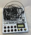
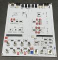
| | + | The prototype consists of two main parts: A top PCB with gold-plated through-hole sockets suitable for |
| | + | 2 mm patch cables, and a base PCB, which contains the main electronic circuitry, the |
| | + | manual controls and ports for external connectivity. A [[Panel Meter]] mounted in the top PCB can be used to display coefficient values and, when the device is set to the repetitive operation mode, its operation time. |
| | + | |
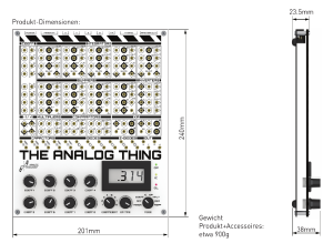
| | + | The size of the analog computer is 203mm x 240mm x 35 mm (with knobs). |
| | + | |
| | <gallery> | | <gallery> |
| | File:Promo 1.jpg|A first glance | | File:Promo 1.jpg|A first glance |
| | File:Front Board v1.0.jpg|Front board v1.0 | | File:Front Board v1.0.jpg|Front board v1.0 |
| | File:Base Board v1.0 patched.jpg|Base board v1.0 | | File:Base Board v1.0 patched.jpg|Base board v1.0 |
| − | File:Test Circuit closeup v1.0.jpg|Some test circuit closeup | + | File:Test Circuit closeup v1.0.jpg|Close-up of a test circuit |
| | </gallery> | | </gallery> |
| | | | |
| − | == Assembly instructions == | + | == Schematics == |
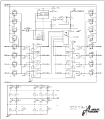
| − | The following sections describe the assembly process of The Analog Thing with BASE board revision 1.0, 04.2021. This board has some minor quirks that must be taken care of as described in the following. | + | The schematics and bill of materials for the base board are [[Open Source]] and can be found here: [https://github.com/anabrid/the-analog-thing] |
| | | | |
| − | Basically the assembly process is straightforward based on the [[:File:Bill_Of_Materials.pdf|bill of materials]] and is straightforward. The BASE printed circuit board should by assembled according to the following steps:
| + | <gallery> |
| | + | File:anathing_v1.2_base_1.png|BASE part 1 |
| | + | File:anathing_v1.2_base_2.png|BASE part 2 |
| | + | File:anathing_v1.2_base_3.png|BASE part 3 |
| | + | File:anathing_v1.2_base_4.png|BASE part 4 |
| | + | File:anathing_v1.2_base_5.png|BASE part 5 |
| | + | File:anathing_v1.2_base_BOM.pdf|Bill of materials BASE |
| | + | </gallery> |
| | | | |
| − | * First, solder in all resistors, capacitors, inductors, transistors, and diodes but leave out R120, R24, R25, D1 and C26, C28, C30, C32, C35, C27, C29, C31, C33, C34 (we will come back to these later). (A nice introduction to soldering SMD parts by hand can be found at [[https://josepheoff.github.io/posts/howtosolder-11soldersmdpassive]] or at [[https://mansfield-devine.com/speculatrix/2018/05/adventures-in-smd-soldering-part-1-by-hand/]].) It is advisable to solder in each type of component at a time. All parts denoted with a * in the bill of materials are high precision parts, i.e. resistors with 0.1% of precision etc. '''Attention:''' The positive side of the 47μF capacitors is denoted by the dark stripe on the capacitor! '''Attention:''' The markings for C5 are the wrong way around on the PCB! The dark stripe of C5 must point upwards to the connector end of the BASE board!
| + | The schematic of the FRONT PCB can be found here: |
| − | * In the next step, solder in IC2 (LM4040x) and all connectors except the 1x4 pinhead for the connection of the panel voltmeter (we will come to this later, too). Please note that the rear connector of the Cinch connectors must be trimmed slightly with a side-cutter as the through hole in the PCB is a tad to small.
| |
| − | * The next step involves soldering in the DC/DC-converter IC1 (TBA2-0522).
| |
| − | * Solder in switch J12 (lower right).
| |
| − | * Solder in the trim resistor R14.
| |
| | | | |
| − | Having finished these tasks, the first test can be performed:
| + | <gallery> |
| − | | + | File:anathing_v1.2_front_1.png|FRONT part 1 |
| − | * Set the switch J12 to its second position from the fully counter clockwise position (this is OFF).
| + | File:anathing_v1.2_front_2.png|FRONT part 2 |
| − | * Connect THE ANALOG THING to a suitable 5V source via the USB cable.
| + | File:anathing_v1.2_front_BOM.pdf|Bill of materials FRONT |
| − | * Now switch J12 to its fully counter clockwise position (this is MINION mode which implicitly turns on the circuit).
| + | </gallery> |
| − | * check that all supply voltages are present and valid:
| |
| − | ** Check for -12V at pin 11 of IC25.
| |
| − | ** Check for +12V at pin 4 of IC25.
| |
| − | ** Check for +5V at pin 14 of IC23.
| |
| − | ** Check for +5V at the lower left pin of IC2.
| |
| − | | |
| − | If these tests turn out to be OK, the rest of the board can be populated with parts:
| |
| − | | |
| − | * Solder in all remaining ICs.
| |
| − | * Solder in 1nF WIMA PP capacitors as C26, C28, C30, C32, and C35. These are the integration capacitors for the large time scale factor of the integrators. The result should look as follows: [[File:1nF_WIMA.jpg|500px]]
| |
| − | * Solder in the five 100nF capacitors C27, C29, C31, C33, C34 in the lower part of the PCB: [[File:100nF.jpg|500px]]
| |
| − | * Now it is time to solder in switch J11, and the potentiometers R16-R23 and the potentiometer R100. '''Attention:''' R100 is a 100k potentiometer with a logarithmic (!) curve while the potentiometers R16-R23 have a linear resistance curve. These potentiometers look basically identical and can be distinguished by the markings at their back. The potentiometers marked B1 are of the linear type (R16-R23) while the potentiometer marked A2 is the logarithmic potentiometer R100: [[File:lin_log_potentiometers.jpg|500px]]
| |
| − | | |
| − | Now a minor fix must be made to allow for operation of the digital panel voltmeter (DVM). Originally the DVM should have been supplied by the +12V supply of THE ANALOG THING. Unfortunately this does not work since the inputs of the DVM are not referenced to ground (GND). To compensate for this the supply of the DVM must my changed to be symmetrical with respect to ground. By means of two Z-diodes two voltages of about +/-6V are generated which are then used to power the DVM:
| |
| − | | |
| − | * Solder in the 1x4 pinhead J13 but bend up its top pin so that it does not touch the through hole in the PCB.
| |
| − | * Solder in a BZX84 6V2 Z-diode in the place of D1.
| |
| − | * Short circuit the two pins of this Z-diode either with a short wire or with a 0 Ohm resistor.
| |
| − | * Solder a second BZX84 6V2 Z-Diode with its anode to the bottom connection of C60 (as shown below) and connect its cathode with a thin wire to the topmost pin of the 1x4 pinhead connector. The result should look like this: [[File:dvm_patch.jpg|500px]]
| |
| − | * Now it is time to solder the four connector cable to the DVM. In addition this bridge P3 on the back of the DVM must be opened and P1 must be closed to set the decimal point to its correct position: [[File:dvm_connections.jpg|500px]]
| |
| − | * Do not yet connect the DVM to the BASE board. Connect the base board to a USB power supply and turn switch J12 to its leftmost position thus turning THE ANALOG THING on (MINION mode). Now measure the voltage at the top two pins of the 1x4 pinheader for the DVM against ground (one pin at a time). The top most pin should read -6...V while the second pin from top should read +6...V (the exact value is not important, it should be around +/-6V).
| |
| − | | |
| − | There are two additional patches to perform:
| |
| − | * R100 is connected the wrong way around, so the scale does not match the value set. To change this, cut through the two traces connecting the left and right pin of R100. Then connect these two pins with thin patch wires crosswise with the cut traces.
| |
| − | * The fast repetitive mode (REPF) does not work without another tiny change: Cut through the trace leading to pint 6, IC28. Connect pin 6, IC28, with a thin wire to the lower end of R11 as shown below: [[File:patches_2.jpg|500px]]
| |
| − | | |
| − | The remaining steps are:
| |
| − | * Install the four plastic spacers on the BASE board and snap in the pre-drilled plexi-glass sheet.
| |
| − | * Install the four hexagonal spacers in the corners of the BASE board: [[File:base_pcb.jpg|500px]]
| |
| − | * Snap the DVM with its attached four connector cable into the FRONT PCB.
| |
| − | * Connect the DVM cable with the 1x4 pinheader J13.
| |
| − | * Mate FRONT and BASE PCBs (the two 50 pin connectors require some patience as well as some deliberate but careful force to fully close).
| |
| − | * Secure the FRONT PCB with four screws in its corners.
| |
| − | * Plug the knobs to the axes of the switches and potentiometers.
| |
| − | | |
| − | That's it! You should now have a fully working ANALOG THING. :-)
| |
| − | | |
| − | == Testing ==
| |
| − | The next step should be to test your ANALOG THING thoroughly.
| |
| | | | |
| − | * Adjust the DVM and check the coefficient potentiometers:
| + | == CAD and Gerber files == |
| − | ** First of all, set the mode control switch on the bottom right to OFF.
| + | {{Todo|Upload the Gerber files here}} |
| − | ** Connect THE ANALOG THING to a 5V USB power supply by means of a USB-A/USB-A cable.
| |
| − | ** Set the mode control switch to COEFF. In this mode the coefficient potentiometers can be set with the DVM showing the current value of any of the eight coefficient potentiometers COEFF 1..COEFF 8.
| |
| − | ** Set the COEFFICIENT switch to 1.
| |
| − | ** Set the potentiometer COEFF 1 fully counter clockwise. The DVM should now display zero (a slight deviation from zero is permissible, so a displayed value of 0.003 would be OK, too).
| |
| − | ** Now turn the potentiometer COEFF 1 fully clockwise.
| |
| − | ** Adjust R14 (right side of THE ANALOG THING) with a tiny screw driver until the DVM displays 1.000.
| |
| − | ** Check the remaining potentiometers by stepping the COEFFICIENT switch through positions 2 to 8 while setting each of the remaining potentiometers first fully counter clockwise and then fully clockwise. The DVM should display (nearly) zero and 1.000 in these two cases.
| |
| | | | |
| − | * Test the summers and inverters:
| + | [[File:THAT-Dimensions.png|thumb|A first glance at the dimensions of THAT]] |
| − | ** Set the mode switch to IC (initial condition).
| |
| − | ** The following steps are to be performed for each of the foud summers:
| |
| − | *** Connect the jack labelled U on the front panel with one of the output jacks of the summer being tested. Connect one of the inputs with weight 1 with the machine unit -1 (lower left corner of the patch field). The DVM should display a value very near to +1.000.
| |
| − | *** Connect the -1 machine unit shortly with one of the summer inputs weighted with 10. The DVM must show a value in excess of 1.100 and the overload indicator OL should be lit.
| |
| − | ** Perform the first of these steps with each of the four inverters. (Do not connect -1 or +1 directly to the summing junction input SJ.)
| |
| | | | |
| − | * Test the multipliers (perform the following steps for each of the two multipliers available on the analog computer):
| + | The size of the PCB is 201mm x 240mm. The overall height (including feet and front panel potentiometers) is 38mm. The height of the two PCBs (without screws) is 16mm. Note that the base PCB has throught hole components, thus feets are mandatory (at least 2mm in elevation). The weight is approximately 900g including cables. |
| − | ** Connect the DVM to the output of the multiplier being tested.
| |
| − | ** Connect the two inputs of the multiplier with +1 and +1 and check that the DVM reads very near to 1.000.
| |
| − | ** Connect the two inputs of the multiplier with -1 and -1 and check that the DVM reads very near to +1.000.
| |
| − | ** Connect one input to +1 and one input to -1. The DVM should now read very near to -1.000.
| |
| | | | |
| − | * Test the comparators (perform the following steps for each of the two comparators):
| + | We have digital [[3D Models of The Analog Thing]] in the wiki. |
| − | ** Connect the >0 input with +1 and the <0 input with -1.
| |
| − | ** Connect the DVM with the OUT jack of the comparator.
| |
| − | ** Connect either A or B with +1 and then with -1. The DVM display must switch between near +1.000 and -1.000.
| |
| | | | |
| − | * Test the integrators (perform the following steps for each of the five integrators):
| + | == Instructions and further reading == |
| − | ** Make sure the mode switch is set to initial condition (IC).
| |
| − | ** Connect -1 to the IC input of the integrator.
| |
| − | ** Connect the DVM (the jack labelled U) with the output of the integrator.
| |
| − | ** Check that the DVM shows near +1.000. With IC connected to +1 instead, the DVM should read near -1.000. If this is the case, IC mode works.
| |
| − | ** Connect the jack labelled SLOW with OUT of the integrator under test, thus selecting a low time scale factor.
| |
| − | ** Connect the IC jack with +1, and connect one of the inputs with weight 1 with -1.
| |
| − | ** The DVM should now read near -1.000.
| |
| − | ** Set the mode selector switch to operate (OP). The DVM display should now increase quickly from about -1.000 to > 1.000 and the overload indicator OL will be lit.
| |
| | | | |
| − | A more thorough test of the integrators can (and should) be done with an external oscilloscope or a sound card "oscilloscope" as follows:
| + | * [[Assembly instructions]] |
| − | * This test requires two integrators and one inverter.
| + | * [[Testing]] instructions |
| − | * Set the mode select switch to initial condition (IC).
| + | * [[Components of The Analog Thing]] |
| − | * Connect the slow jack of each of the two integrators with an output jack of the very same integrator, thus selecting a low time scale factor.
| + | * [[The Analog Thing FAQ]] |
| − | * Connect IC of the 1st integrator (I1) to +1. | |
| − | * Connect the output of I1 with an input with weight 1 of the 2nd integrator (I2). | |
| − | * Connect the output of I2 with the input of an inverter. | |
| − | * Connect the output of that inverter with an input with weight 1 of I1. (This circuit now solves the differential equation y'' = -y.)
| |
| − | * Connect the output of I1 with the jack labelled X.
| |
| − | * Connect the X output at the back of THE ANALOG THING with an oscilloscope or a sound card input (some oscilloscope software is assumed to be up and running on your computer).
| |
| − | * The oscilloscope should display a line at -1 (the output jacks are fed by a voltage divider so the actual reading is less than the machine unit voltage of -10V - this was done to avoid damage to an attached sound card).
| |
| − | * Set the mode selector switch to operate (OP). The oscilloscope will now display a rather low frequency sine curve.
| |
| − | * Set the mode selector switch back to IC and remove the two connections between SLOW and the OUT jack of each of the two integrators.
| |
| − | * Set the mode selector to OP. The oscilloscope should now display a sine wave with much higher frequency (factor 100) than before. (This signal's amplitude may increase or decrease over time which is normal and more or less unavoidable in a simple setup like this.) | |
| | | | |
| − | The only thing left to test is the repetitive mode of operation:
| + | [[Category:Manual]] |
| − | * Turn the potentiometer labelled OP-TIME fully counter clockwise.
| |
| − | * Set the mode selector switch to REP.
| |
| − | * The LEDs OP and IC should be flickering.
| |
| − | * Slowly turning the OP-TIME potentiometer clockwise should cause the OP indicator light for longer and longer periods of time.
| |
| − | * Perform this test also with the mode selector switch in REPF (fast repetitive mode).
| |
